Description:
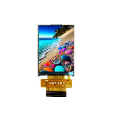
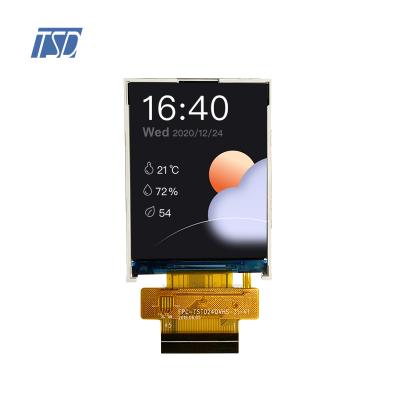
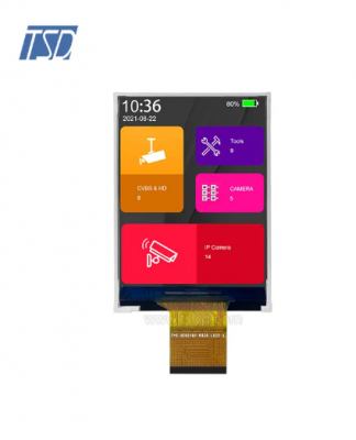
TST024QVHI-17P is 2.4 inch 240x320 resolution MCU/SPI/SPI+RGB LCD display module, with standard resistive touch panel. Backlight is 300 nits, White LEDs is 3, backlight current is 20mA and backlight voltage is 12V, which could be customized. For this 2.4 inch TFT LCD module, driver IC is ILI9341V, viewing direction is free, all o'clock, color depth is 65K, white backlight and transmissive mode.
Drawing:

Specifications:
| General Specification | ||
| Part No. | TST024QVHI-17P | |
| Outline Dimension(mm) |
42.72x59.46x3.4 |
|
| Active Area(mm) | 36.72x48.96 | |
| Resolution(dots) | 240x320 | |
| Operating temperature(°C) | -20 ~ +70°C | |
| Storage temperature(°C) | -30 ~ +80°C | |
| Number of Pixel(pixels) | 240(H)xRGBx320(V) | |
| Touch panel | with RTP | |
| Driver IC | ILI9341V | |
| Pixel arrangement | RGB-stripe | |
| Display mode | Normal black,IPS, 2.4 inch TFT | |
| Surface treatment | Antiglare | |
| View direction | All |
|
| Weight(g) | TBD | |
| Power Consumption(w) | Panel | TBD(Typ.) |
| B/L system | TBD(Typ.) | |
| Interface | MCU/SPI/SPI+RGB |
|
| Module lifetime(Hours) | 30,000-40,000 | |
| Pins Description | ||
| Pin No. | Symbol | Description |
| 1 | NC | No connect. |
| 2-5 | IM0-IM3 | Interface selection |
| 6 | RESET | This signal will reset the device and must be applied to properly initialize the chip. Signal is active low. |
| 7 | VSYNC | Frame synchronizing signal for RGB innterface operation. |
| 8 | HSYNC | Line synchronizing signal for RGB interface operation. |
| 9 | DOTCLK | Dot clock signal for RGB iterface operation. |
| 10 | ENABLE | Data enable signal for RGB interface operation |
| 11-28 | DB17-DB0 | 18-bit parallel bi-directional data bus for MCU system and RGB interface mode. |
| 29 | SDO | Serial output signal. |
| 30 | SDI | When IM[3]: low, serial in/out signal, When IM[3]: High, serial input signal. The data is applied on the rising edge on the rising edge of the SCL signal |
| 31 | RD | 8080-I/8080-II system (RD): serves as a read signal and MCU read data at the rising edge. |
| 32 | RS/SCL | This pin is used to select "Data or Command" in the parallel interface or 4-wire 8 bit serial data interface. When RS=1, data is selected. When RS=0, command is selected. This pin is used serial interface clock in 3-wire 9-bit / 4-wire 8-bit serial data in interface. |
| 33 | WR/RS | 8080-I/8080-II system(WR): serves as a write signal and writes data at the rising edge. 4 line system (RS): serves as command or parameter select. |
| 34 | CS | Chip select signal |
| 35 | FMARK | Tearing effect output pin to synchronize MPU to frame writing, activated by S/W command. When this pin is not activated, this pin is low. |
| 36-37 | VCC | Power supply +2.8V |
| 38-39 | GND | System ground. |
| 40 | LEDA | Backlight A Anode input pin |
| 41 | LEDK | Backlight K Cathode input pin |
| 42 | XR | The touch panel X right pin. |
| 43 | YD | The touch panel Y down pin. |
| 44 | XL | The touch panel X right pin. |
| 45 | YU | The touch panel Y up pin. |
Applications:
For our 2.4 inch LCD display TST024QVHI-17P, is with resistive touch panel, could be used in electronic toys, also used in smart home product, such as smart thermostat, temperature and humidity control panel.

Product Features:
This display module is a transmissive type color active matrix TFT(Thin Film Transistor) liquid crystal display (LCD) that could be used in many applications. This module is composed of a FOG, a driver-circut, and a back-light unit.The resolution of a 2.4" contains 240x320 dots and can display up to 65k colors.
 Email : info@tslcd.com
 Tel : +86-755-28225963


